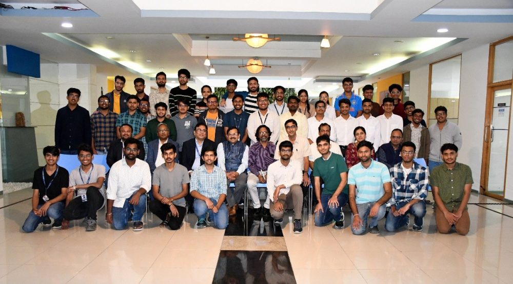
The Samsung chip design studio was launched at IIIT-Bangalore. The studio was inaugurated by Mr. Balajee Sowrirajan, EVP & MD, SSIR, alongside Prof. Debabrata Das, Director, IIIT-B, in the presence of esteemed faculty, industry experts, and students.
Set up in collaboration with Samsung Semiconductor India Research (SSIR), this state-of-the-art facility is equipped with EDA tools to make chip design accessible to students and early-career engineers. This initiative, aims to bridge the gap between academic learning and industry demands by providing hands-on training in circuit design, simulation, and characterization. The facility will serve as a launchpad for aspiring VLSI engineers, allowing them to implement, simulate, and validate innovative designs. Selected student teams will gain sponsored access to cutting-edge tools, with expert mentorship from Prof. Madhav Rao, Head of the ECE Department, and a panel of industry specialists. The program will support 10 teams, with the top three projects earning special recognition.